Modular ShieldSigner with a 2.8-inch display
This variant keeps the Plus's 2.8-inch ST7789 display size, smartcard reader and Luckfox processor, while using an assembled LCD board that plugs into ordinary headers. JLCPCB assembles the small components; customer soldering is limited to 2.54 mm through-hole headers. It follows MOD-PROTO's module-based approach without using its smaller 1.3-inch display.
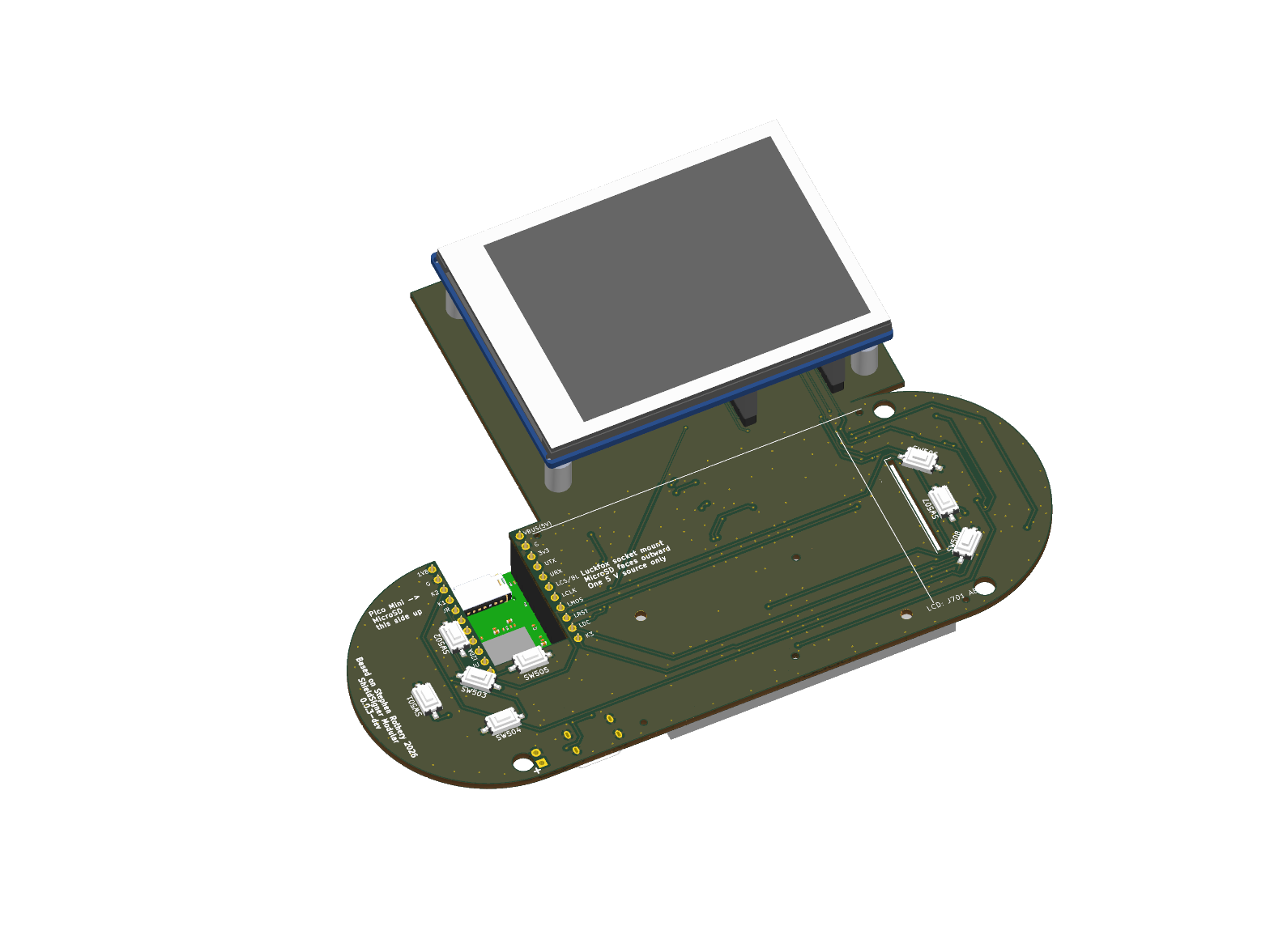
Get the design and order files
- Open the native KiCad project, including local footprints and portable 3D models.
- Download the matched JLCPCB quote kit: inner Gerber ZIP, BOM, CPL, population, customer parts and review notes.
- Assembly and first-power guide, 32-part carrier BOM, placement file, customer shopping list.
- Native check results, mechanical checks, manufacturing readiness, dated stock audit.
- Front copper drawing, back copper drawing, complete STEP assembly, GLB assembly.
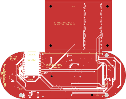
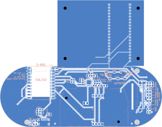
These are prototype quotation files, with clean native ERC/DRC, connectivity and parity checks. The two inherited courtyard exclusions cover unpopulated strap pairs; the checker requires all four straps to remain DNP. No physical board, display fit, powered bring-up or assembler placement preview has been tested. The standard FPC carrier remains separate; its BOM/CPL/Gerbers do not apply here.
Display choice and why it works
Buy Waveshare Pico-ResTouch-LCD-2.8, as an assembled display module without a Raspberry Pi Pico CPU. Manufacturer product, pinout and examples, retained schematic.
It provides a 240×320 ST7789 display, its own 3.3 V regulator, LED resistors/backlight transistor and two Pico-format 20-position receptacle rows. The carrier supplies 5 V to VSYS and 3.3 V control signals. The factory handles the panel connection, so the customer does not install a display ribbon or fine-pitch FPC connector. The larger module has no navigation buttons: all eight carrier buttons remain fitted. Touch and the module's extra SD slot are unused.
This is not the Waveshare 2.8-inch DSI display, the 1.3-inch LCD HAT, or an ESP32/RP2350 display board. The signer CPU remains the Luckfox Pico Mini. The camera still uses its direct Luckfox ribbon connection.
The manufacturer's STEP and dimension photograph agree on 70.2×52.2 mm, despite the product table saying 50.2 mm. The board uses the STEP envelope and its four mounting centers. The Pico interface uses nominal 17.78 mm row spacing and 2.54 mm pitch; the supplied STEP depicts 17.80 mm between header centers, a 0.02 mm discrepancy retained in the model rather than distorting it. Confirm the purchased module revision during the first fit test.
The carrier is approximately 137.86×108.58 mm: it reserves a separate display bay above the inherited electronics, keeping header pins clear of the smartcard socket. It needs a new enclosure. This favors accessible, ordinary connectors and a mechanically supported module over minimizing board size.
Header wiring
J701 uses the display's Pico physical pin numbers, not Luckfox pin numbers. Its carrier-top view mirrors the manufacturer's rear view. Pin 1 is the square pad; the marked USB end points toward the top of the display bay.
| J701 module pin | Function | Carrier connection | Purpose |
|---|---|---|---|
| 39 | VSYS | +5V | Supplies the module regulator and display |
| 3, 8, 13, 18, 23, 28, 33, 38 | Grounds | GND | Power and signal return |
| 11 / GP8 | LCD_DC | LCD_DC; Luckfox 10 | Commands versus pixel data |
| 12 / GP9 | LCD_CS | RPI_SPI_CS; default jumper path to Luckfox 6 | SPI selection |
| 14 / GP10 | LCD_CLK | LCD_SCLK; Luckfox 7 | SPI clock |
| 15 / GP11 | MOSI | LCD_MOSI; Luckfox 8 | Commands and RGB565 pixels |
| 20 / GP15 | LCD_RST | LCD_RST; Luckfox 9 | Hardware reset |
| 17 / GP13 | LCD_BL | +3.3V | Enables onboard backlight transistor; always on |
| 21 / GP16 | TP_CS | +3.3V | Deselects unused touch controller |
| 29 / GP22 | SD_CS | +3.3V | Deselects unused module SD interface |
| 36 / Pico3V3 | Optional Pico supply | No connection | Avoids joining the carrier and module regulator outputs |
| All others | Unused GPIO, readback, touch, SD, VBUS, RUN | Explicit no-connect | No extra CPU or peripheral functionality wired |
The display's onboard regulator supplies its LCD load rather than drawing that load from the Luckfox 3.3 V output. The BL input drives an onboard 1 kΩ base resistor and transistor; four 10 Ω LED branches are already on the module. The manufacturer FAQ quotes 5 V/140 mA maximum module power consumption. This is supplier information, not a measured whole-signer budget; verify rail droop with camera and smartcard operations.
Keep JP203 and JP205 closed, JP204 and JP206 open for chip select. JP201/JP202 do not control this module's backlight. Do not select the old alternative PWM/permanently-selected configuration. J401, C401, Q401 and R401–R410 are DNP; their inherited lands receive no reflow paste. J302 also stays DNP. The retained old mode-strap footprints have no role in configuring the purchased module.
Assembly and manufacturing
The matched kit has 32 SMT placements and 16 JLC catalog lines, with eight top-side switches and the remaining circuitry on the bottom. All 16 part identities currently have SMT assembly catalog entries; the dated snapshot supports a five-board prototype quote. The limiting stock fields were 28 smartcard sockets and 55 SEC1210/PV-UR2 bridges. Stock is not reserved and final sourcing/placement is confirmed in JLCPCB's quote.
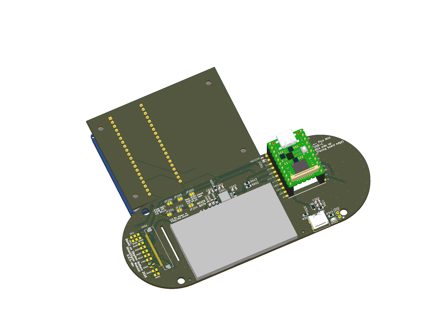
The customer buys the LCD, Luckfox and headers separately. J701 is two 1×20 male strips, with the rows 17.78 mm apart, not an ordinary tightly spaced 2×20 header. The Luckfox mount uses two 1×11 sockets and, unless already fitted, two male strips on the module. No QFN, USB-C signal pins or smartcard contacts need customer soldering.
The selected Amphenol 7312P0225A13LF is a full-size contact smartcard socket. Use an appropriate full-size adapter for a compatible SIM-size card; the footprint name inherited from upstream does not make this a second independently fitted SIM socket. Card firmware/application compatibility still follows the smartcard guide.
Footprints and 3D models
The modular variant has dedicated reflow footprints for the selected XKB switch, SHOUHAN USB connector, Amphenol socket and Microchip SEC1210. Supplier drawings define their pad sizes/centers. Native checks independently assert these dimensions and the display/host header geometry. The SEC1210 uses 0.35 mm-wide, 0.65 mm-long lead lands, a 4.0 mm inner gap, and retains its 3.4 mm exposed-pad land and four reduced paste windows; its datasheet specifies a 3.3 mm nominal/3.4 mm maximum package exposed pad.
Seventeen local STEP models have provenance and SHA-256 checks. There are no workstation-specific or missing active model paths. The display is the manufacturer's complete STEP; the host, selected switch and USB/bridge representations are retained supplier/upstream models. The card socket is a simplified dimensional envelope and the spacer model omits threads—neither is presented as detailed manufacturer CAD. DNP parts are omitted from the assembled views.
The modeled display PCB back is 12 mm above the carrier, using its 4 mm factory bosses plus specified 8 mm extensions. The male posts engage the modeled female headers by about 5.54 mm. The Luckfox stack accounts for both 8.5 mm socket housings and 2.54 mm male header insulators. See assembly measurements and steps before selecting hardware; do not assume the included display spacers have the required length.
Reproduce checks and outputs
Run from the repository root:
git lfs pull
mise run variant:lcd:check
mise run variant:lcd:models
mise run variant:lcd:fab
mise run variant:lcd:review
mise run variant:lcd:package
check runs ERC/DRC/parity and header/population assertions. models verifies local model hashes, mounting centers and reviewed solder lands. fab creates a matched prototype quote kit with its own native placement export and common Gerber/drill/CPL origin. review generates STEP/GLB and assembled renders. package bundles the portable project and pins release checksums after those outputs are generated. The experimental tscircuit view still describes the separate standard carrier.
MOD-PROTO's local hardware guide and Python driver establish its assembled 1.3-inch ST7789 HAT approach. A search of the local monorepo's KiCad/Eagle files did not locate a separate MOD-PROTO PCB. No private MOD-PROTO configuration or source is published here.
Source: docs/LCD-MODULE-VARIANT.md ↗. Documentation describes reviewed evidence; it does not replace physical testing.